Decoding ICE40
══════════════
══════════
══════
══
July 26, 2025
Background
══════════
• Forth 2023 gifted a pico-ice by Christopher Lozinski
- Raspberry Pi Pico (RP2040) + iCE40UP5K FPGA
- 4MB SPI Flash for CPU
- 4MB SPI Flash for FPGA
- 8MB low power qSPI RAM
- Shared RGB LED, All RP2040 + iCE40 pins exposed
- RP2040 can feed configuration to FPGA!
• By December ported uEforth
- and ability to send an FPGA image
So what next?
═════════════
• Wouldn't it be cool to interactively create gates?
• Toolchains, even open source ones are slow
icestorm/YoSYS
══════════════
• Community has reverse engineered
the iCE40 bitstream format!
• Built an open source verilog
• icepack capture fairly simple config layout
https://prjicestorm.readthedocs.io/en/latest/format.html
Time passes...
More time passess...
What's taking so long?
══════════════════════
• Better understand the mapping between bits and routing
• Some progress on simulation
BUT...
• Strugged to unravel + simplify open source representation
- things are represented as data instead of code
• Realized routing constraints may fail fairly easily
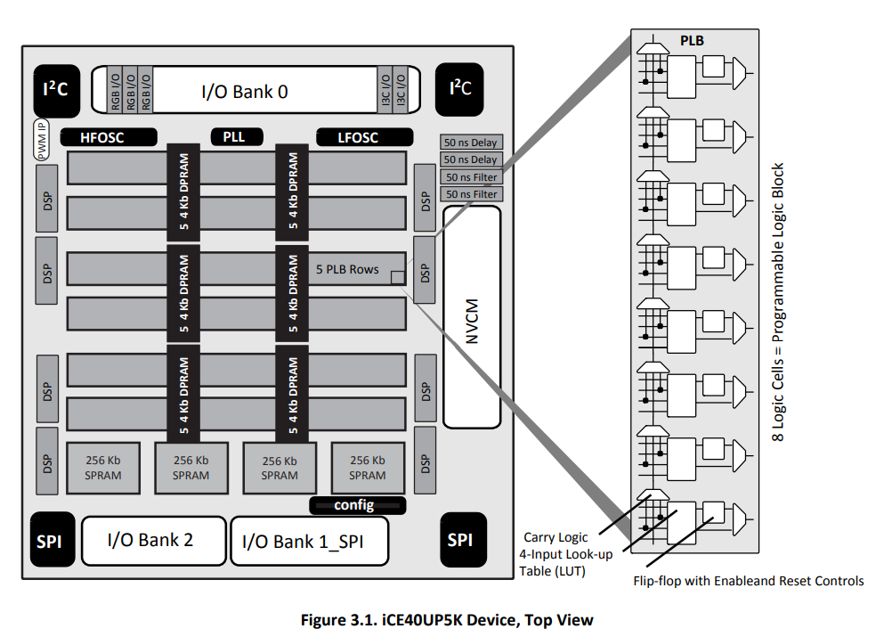
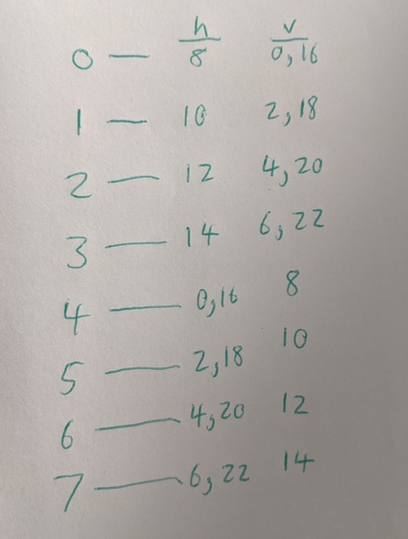
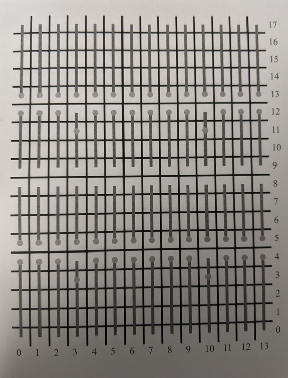
iCE40UP5K
═════════
• 5280 LUTs
• 1Mbit single port RAM
• 120Kb dual port RAM
• 8 x DSP blocks
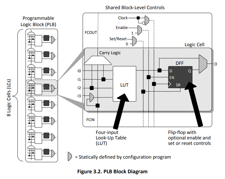
@ice40-top.png
 @ice40-plb.png
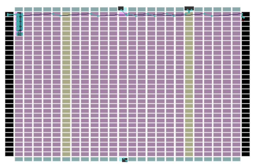
 @ice40-viewer.png
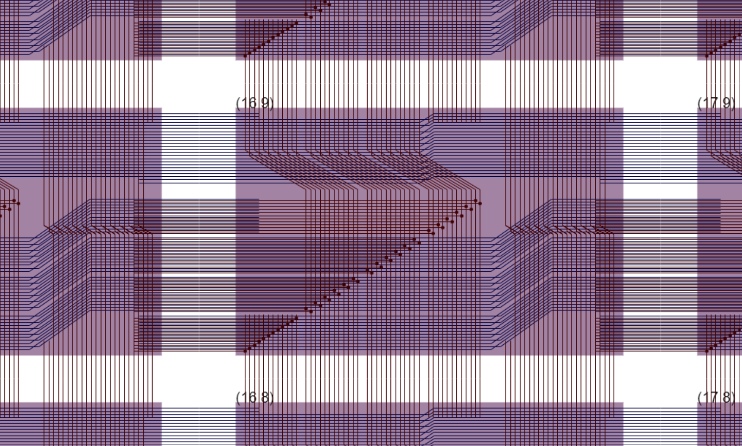
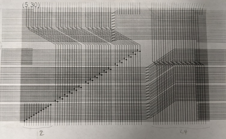
 @ice40-spans.png
 @arouting1.jpg
 https://knielsen.github.io/ice40_viewer/ice40_viewer.html
iCE40 Format
════════════
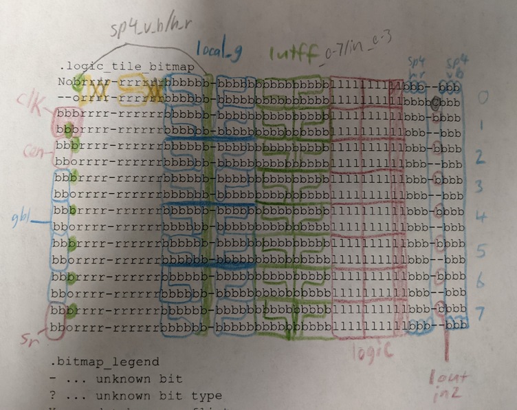
• icepack capture fairly simple config layout:
if (right_half)
cram_x = bank_xoff + column_width - 1 - bit_x;
else
cram_x = bank_xoff + bit_x;
if (top_half)
cram_y = bank_yoff + (15 - bit_y);
else
cram_y = bank_yoff + bit_y;
.logic_tile_bitmap
Nobrrrr-rrrrrrbbbbbb-bbbbbbbbbbbbbbbllllllllllbbb--bbb
--orrrr-rrrrrrbbbbbb-bbbbbbbbbbbbbbbllllllllllbbbbCbbb
bbbrrrr-rrrrrrbbbbbb-bbbbbbbbbbbbbbbllllllllllbbb-bbbb
bbbrrrr-rrrrrrbbbbbb-bbbbbbbbbbbbbbbllllllllllbbb--bbb
bbbrrrr-rrrrrrbbbbbb-bbbbbbbbbbbbbbbllllllllllbbb-bbbb
bborrrr-rrrrrrbbbbbb-bbbbbbbbbbbbbbbllllllllllbbb--bbb
bbbrrrr-rrrrrrbbbbbb-bbbbbbbbbbbbbbbllllllllllbbb-bbbb
bborrrr-rrrrrrbbbbbb-bbbbbbbbbbbbbbbllllllllllbbb--bbb
bbbrrrr-rrrrrrbbbbbb-bbbbbbbbbbbbbbbllllllllllbbb-bbbb
bborrrr-rrrrrrbbbbbb-bbbbbbbbbbbbbbbllllllllllbbb--bbb
bbbrrrr-rrrrrrbbbbbb-bbbbbbbbbbbbbbbllllllllllbbb-bbbb
bborrrr-rrrrrrbbbbbb-bbbbbbbbbbbbbbbllllllllllbbb--bbb
bbbrrrr-rrrrrrbbbbbb-bbbbbbbbbbbbbbbllllllllllbbb-bbbb
bborrrr-rrrrrrbbbbbb-bbbbbbbbbbbbbbbllllllllllbbb--bbb
bbbrrrr-rrrrrrbbbbbb-bbbbbbbbbbbbbbbllllllllllbbb-bbbb
bborrrr-rrrrrrbbbbbb-bbbbbbbbbbbbbbbllllllllllbbb--bbb
- ... unknown bit
r ... routing
b ... buffer
l ... logic bits
o ... ColBufCtrl
C ... CarryInSet
N ... NegClk
@tilebits1.jpg
https://knielsen.github.io/ice40_viewer/ice40_viewer.html
iCE40 Format
════════════
• icepack capture fairly simple config layout:
if (right_half)
cram_x = bank_xoff + column_width - 1 - bit_x;
else
cram_x = bank_xoff + bit_x;
if (top_half)
cram_y = bank_yoff + (15 - bit_y);
else
cram_y = bank_yoff + bit_y;
.logic_tile_bitmap
Nobrrrr-rrrrrrbbbbbb-bbbbbbbbbbbbbbbllllllllllbbb--bbb
--orrrr-rrrrrrbbbbbb-bbbbbbbbbbbbbbbllllllllllbbbbCbbb
bbbrrrr-rrrrrrbbbbbb-bbbbbbbbbbbbbbbllllllllllbbb-bbbb
bbbrrrr-rrrrrrbbbbbb-bbbbbbbbbbbbbbbllllllllllbbb--bbb
bbbrrrr-rrrrrrbbbbbb-bbbbbbbbbbbbbbbllllllllllbbb-bbbb
bborrrr-rrrrrrbbbbbb-bbbbbbbbbbbbbbbllllllllllbbb--bbb
bbbrrrr-rrrrrrbbbbbb-bbbbbbbbbbbbbbbllllllllllbbb-bbbb
bborrrr-rrrrrrbbbbbb-bbbbbbbbbbbbbbbllllllllllbbb--bbb
bbbrrrr-rrrrrrbbbbbb-bbbbbbbbbbbbbbbllllllllllbbb-bbbb
bborrrr-rrrrrrbbbbbb-bbbbbbbbbbbbbbbllllllllllbbb--bbb
bbbrrrr-rrrrrrbbbbbb-bbbbbbbbbbbbbbbllllllllllbbb-bbbb
bborrrr-rrrrrrbbbbbb-bbbbbbbbbbbbbbbllllllllllbbb--bbb
bbbrrrr-rrrrrrbbbbbb-bbbbbbbbbbbbbbbllllllllllbbb-bbbb
bborrrr-rrrrrrbbbbbb-bbbbbbbbbbbbbbbllllllllllbbb--bbb
bbbrrrr-rrrrrrbbbbbb-bbbbbbbbbbbbbbbllllllllllbbb-bbbb
bborrrr-rrrrrrbbbbbb-bbbbbbbbbbbbbbbllllllllllbbb--bbb
- ... unknown bit
r ... routing
b ... buffer
l ... logic bits
o ... ColBufCtrl
C ... CarryInSet
N ... NegClk
@tilebits1.jpg
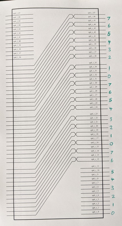
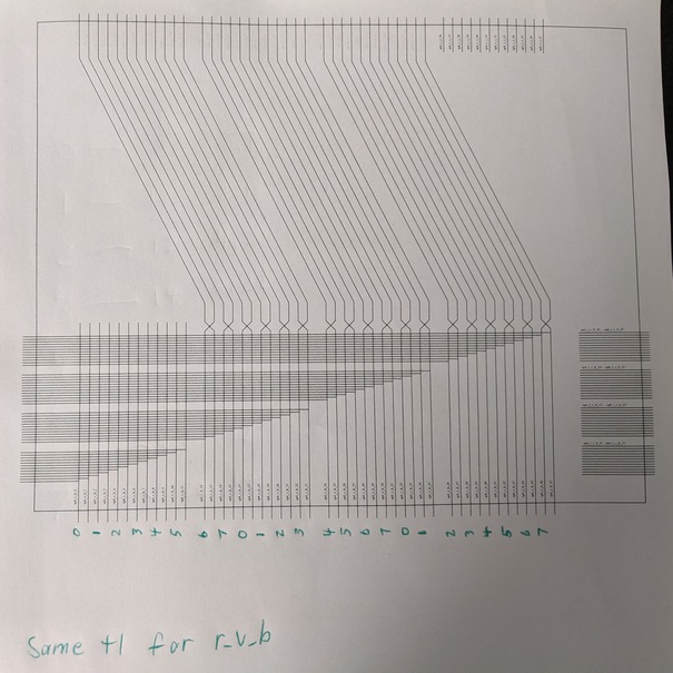
 chipdb-5k.txt
.net 514
0 2 sp4_h_r_0
1 2 sp4_h_r_13
2 2 sp4_h_r_24
3 2 sp4_h_r_37
4 2 sp4_h_l_37
.routing 25 30 103375 B6[11] B6[13] B7[12]
001 86500
010 98041
011 103318
100 86493
101 98040
110 98045
111 103314
.buffer 25 30 103209 B6[14] B7[14] B7[15] B7[16] B7[17]
00001 103357
00011 78827
00101 103265
00111 90387
01001 103344
01011 64134
01111 103317
10011 98042
10101 94028
10111 98431
11001 103257
11011 98176
11101 94151
11111 98441
.logic_tile_bits 54 16
CarryInSet B1[50]
ColBufCtrl.glb_netwk_0 B9[7]
ColBufCtrl.glb_netwk_1 B8[7]
ColBufCtrl.glb_netwk_2 B11[7]
ColBufCtrl.glb_netwk_3 B10[7]
ColBufCtrl.glb_netwk_4 B13[7]
ColBufCtrl.glb_netwk_5 B12[7]
ColBufCtrl.glb_netwk_6 B15[7]
ColBufCtrl.glb_netwk_7 B14[7]
LC_0 B0[36] B0[37] B0[38] B0[39] B0[40] B0[41] B0[42] B0[43] B0[44] B0[45] B1[36] B1[37] B1[38] B1[39] B1[40] B1[41] B1[42] B1[43] B1[44] B1[45]
LC_1 B2[36] B2[37] B2[38] B2[39] B2[40] B2[41] B2[42] B2[43] B2[44] B2[45] B3[36] B3[37] B3[38] B3[39] B3[40] B3[41] B3[42] B3[43] B3[44] B3[45]
LC_2 B4[36] B4[37] B4[38] B4[39] B4[40] B4[41] B4[42] B4[43] B4[44] B4[45] B5[36] B5[37] B5[38] B5[39] B5[40] B5[41] B5[42] B5[43] B5[44] B5[45]
LC_3 B6[36] B6[37] B6[38] B6[39] B6[40] B6[41] B6[42] B6[43] B6[44] B6[45] B7[36] B7[37] B7[38] B7[39] B7[40] B7[41] B7[42] B7[43] B7[44] B7[45]
LC_4 B8[36] B8[37] B8[38] B8[39] B8[40] B8[41] B8[42] B8[43] B8[44] B8[45] B9[36] B9[37] B9[38] B9[39] B9[40] B9[41] B9[42] B9[43] B9[44] B9[45]
LC_5 B10[36] B10[37] B10[38] B10[39] B10[40] B10[41] B10[42] B10[43] B10[44] B10[45] B11[36] B11[37] B11[38] B11[39] B11[40] B11[41] B11[42] B11[43] B11[44] B11[45]
LC_6 B12[36] B12[37] B12[38] B12[39] B12[40] B12[41] B12[42] B12[43] B12[44] B12[45] B13[36] B13[37] B13[38] B13[39] B13[40] B13[41] B13[42] B13[43] B13[44] B13[45]
LC_7 B14[36] B14[37] B14[38] B14[39] B14[40] B14[41] B14[42] B14[43] B14[44] B14[45] B15[36] B15[37] B15[38] B15[39] B15[40] B15[41] B15[42] B15[43] B15[44] B15[45]
NegClk B0[0]
DEMO
Visualizer
@hrouting1.jpg
chipdb-5k.txt
.net 514
0 2 sp4_h_r_0
1 2 sp4_h_r_13
2 2 sp4_h_r_24
3 2 sp4_h_r_37
4 2 sp4_h_l_37
.routing 25 30 103375 B6[11] B6[13] B7[12]
001 86500
010 98041
011 103318
100 86493
101 98040
110 98045
111 103314
.buffer 25 30 103209 B6[14] B7[14] B7[15] B7[16] B7[17]
00001 103357
00011 78827
00101 103265
00111 90387
01001 103344
01011 64134
01111 103317
10011 98042
10101 94028
10111 98431
11001 103257
11011 98176
11101 94151
11111 98441
.logic_tile_bits 54 16
CarryInSet B1[50]
ColBufCtrl.glb_netwk_0 B9[7]
ColBufCtrl.glb_netwk_1 B8[7]
ColBufCtrl.glb_netwk_2 B11[7]
ColBufCtrl.glb_netwk_3 B10[7]
ColBufCtrl.glb_netwk_4 B13[7]
ColBufCtrl.glb_netwk_5 B12[7]
ColBufCtrl.glb_netwk_6 B15[7]
ColBufCtrl.glb_netwk_7 B14[7]
LC_0 B0[36] B0[37] B0[38] B0[39] B0[40] B0[41] B0[42] B0[43] B0[44] B0[45] B1[36] B1[37] B1[38] B1[39] B1[40] B1[41] B1[42] B1[43] B1[44] B1[45]
LC_1 B2[36] B2[37] B2[38] B2[39] B2[40] B2[41] B2[42] B2[43] B2[44] B2[45] B3[36] B3[37] B3[38] B3[39] B3[40] B3[41] B3[42] B3[43] B3[44] B3[45]
LC_2 B4[36] B4[37] B4[38] B4[39] B4[40] B4[41] B4[42] B4[43] B4[44] B4[45] B5[36] B5[37] B5[38] B5[39] B5[40] B5[41] B5[42] B5[43] B5[44] B5[45]
LC_3 B6[36] B6[37] B6[38] B6[39] B6[40] B6[41] B6[42] B6[43] B6[44] B6[45] B7[36] B7[37] B7[38] B7[39] B7[40] B7[41] B7[42] B7[43] B7[44] B7[45]
LC_4 B8[36] B8[37] B8[38] B8[39] B8[40] B8[41] B8[42] B8[43] B8[44] B8[45] B9[36] B9[37] B9[38] B9[39] B9[40] B9[41] B9[42] B9[43] B9[44] B9[45]
LC_5 B10[36] B10[37] B10[38] B10[39] B10[40] B10[41] B10[42] B10[43] B10[44] B10[45] B11[36] B11[37] B11[38] B11[39] B11[40] B11[41] B11[42] B11[43] B11[44] B11[45]
LC_6 B12[36] B12[37] B12[38] B12[39] B12[40] B12[41] B12[42] B12[43] B12[44] B12[45] B13[36] B13[37] B13[38] B13[39] B13[40] B13[41] B13[42] B13[43] B13[44] B13[45]
LC_7 B14[36] B14[37] B14[38] B14[39] B14[40] B14[41] B14[42] B14[43] B14[44] B14[45] B15[36] B15[37] B15[38] B15[39] B15[40] B15[41] B15[42] B15[43] B15[44] B15[45]
NegClk B0[0]
DEMO
Visualizer
@hrouting1.jpg
 @vrouting1.jpg
 @vrrouting1.jpg
 Issues...
═════════
• Haven't tackled IO at all
• Haven't looked at PLL setup
• Haven't figured out how globals are routed
@globals1.jpg
Issues...
═════════
• Haven't tackled IO at all
• Haven't looked at PLL setup
• Haven't figured out how globals are routed
@globals1.jpg
 Simuation
═════════
• Model how I'll synthesize once I have all the encoding
• Initially is memory wasteful
- need to use FPGA bit space instead of allocated structures
Goals
═════
• Support talking about multiple wires at once
BUS ( wire bus -- bus' )
UNBUS ( bus' -- wire bus )
• Support allocating registers
8 REGISTER ( bus )
• Support multi-bit logic and arithmetic
x y + z REG!
• Support clocks and enabling
ready ENABLE ! clk1 CLOCK ! x y + z REG!
variable zero
variable one -1 one !
variable luts
variable ffs
variable clock zero clock !
variable enable one enable !
struct lut
cell field ->value
cell field ->next
cell field ->i0
cell field ->i1
cell field ->i2
cell field ->i3
cell field ->table
struct ff
cell field ->value
cell field ->next
cell field ->in
cell field ->enable
cell field ->clock
cell field ->old-clock
: LUT4 { i0 i1 i2 i3 tbl -- o }
here 0 , luts @ , i0 , i1 , i2 , i3 , tbl , dup luts ! ;
: lut-vals { l -- v } l ->i0 @ @ 0<> 1 and
l ->i1 @ @ 0<> 2 and or
l ->i2 @ @ 0<> 4 and or
l ->i3 @ @ 0<> 8 and or ;
: tick-lut { l -- } l ->table @ l lut-vals rshift 1 and 0<> l ->value ! ;
: tick-luts luts @ begin dup while dup tick-lut ->next @ repeat drop ;
: FFL ( -- o )
here 0 , ffs @ , zero , enable @ , clock @ , 0 , dup ffs ! ;
: FF! ( v ff -- ) ->in ! ;
: tick-ff { f -- } f ->clock @ @ 0<> f ->old-clock @ 0= and if
f ->enable @ @ if
f ->in @ @ 0<> f ->value !
then
then
f ->clock @ @ f ->old-clock !
;
: tick-ffs ffs @ begin dup while dup tick-ff ->next @ repeat drop ;
: tick tick-luts tick-ffs ;
: ticks ( n -- ) 0 ?do tick loop ;
: XOR1 ( a b -- o ) zero zero $6666 LUT4 ;
: OR1 ( a b -- o ) zero zero $eeee LUT4 ;
: AND1 ( a b -- o ) zero zero $8888 LUT4 ;
: INVERT1 ( a b -- o ) zero zero zero $aaaa LUT4 ;
: HA ( x y -- so co ) 2dup AND1 >r XOR1 r> ;
: FA ( x y z -- so co ) HA >r HA r> OR1 ;
: BUS ( v bus -- bus ) here >r , , r> ;
: UNBUS ( bus -- v bus ) dup cell+ @ swap @ ;
: nBUS ( v* n -- bus ) 0 swap 0 ?do BUS loop ;
: nUNBUS ( bus -- v* ) begin dup while UNBUS repeat drop ;
: BUS. ( bus -- ) begin dup while UNBUS >r @ . r> repeat drop ;
: BUS! ( n bus -- ) begin dup while
UNBUS >r over 1 and 0<> swap ! 2/ r>
repeat 2drop ;
: INVERT ( a -- a' )
dup 0= if exit then
UNBUS >r INVERT1 r> recurse BUS
;
: AND ( a b -- c )
dup 0= if nip exit then
UNBUS >r >r UNBUS r> swap >r AND1
r> r> recurse BUS
;
: OR ( a b -- c )
dup 0= if nip exit then
UNBUS >r >r UNBUS r> swap >r OR1
r> r> recurse BUS
;
: XOR ( a b -- c )
dup 0= if nip exit then
UNBUS >r >r UNBUS r> swap >r XOR1
r> r> recurse BUS
;
: +c ( a b ci -- c )
>r dup 0= if 2drop r> 0 BUS exit then r>
-rot
UNBUS >r >r UNBUS r> swap >r FA
r> r> rot recurse BUS
;
: + ( a b -- c ) zero +c ;
: REGISTER ( n -- bus )
0 swap 0 ?do FFL swap BUS loop ;
: REG! ( v a -- )
dup 0= if 2drop exit then
UNBUS >r >r UNBUS r> swap >r FF!
r> r> recurse
;
DEMO
Mapping to FPGA CRAM
════════════════════
• Sentinels for: No-connection, globals
• Instead of allocating LUTs + FFs,
encode in FPGA space: bit + x * 8 + y * WIDTH * 8
- CRAM has: Truth Table, 2 layer input route
- For simulation keep bit for each LUT and FF,
one bit to track enable state per PLB
• Handle carry as a special case adder structure?
• How to use the LUT in front of a FF? Waste a LUT per FF?
What's Next?
════════════
• Bite the bullet and allocate paths greedily
• Bootstrap with known good IO pins
• Implement the required checksum + write order
• Lots of debugging...
QUESTIONS❓
🙏
Thank you!
Simuation
═════════
• Model how I'll synthesize once I have all the encoding
• Initially is memory wasteful
- need to use FPGA bit space instead of allocated structures
Goals
═════
• Support talking about multiple wires at once
BUS ( wire bus -- bus' )
UNBUS ( bus' -- wire bus )
• Support allocating registers
8 REGISTER ( bus )
• Support multi-bit logic and arithmetic
x y + z REG!
• Support clocks and enabling
ready ENABLE ! clk1 CLOCK ! x y + z REG!
variable zero
variable one -1 one !
variable luts
variable ffs
variable clock zero clock !
variable enable one enable !
struct lut
cell field ->value
cell field ->next
cell field ->i0
cell field ->i1
cell field ->i2
cell field ->i3
cell field ->table
struct ff
cell field ->value
cell field ->next
cell field ->in
cell field ->enable
cell field ->clock
cell field ->old-clock
: LUT4 { i0 i1 i2 i3 tbl -- o }
here 0 , luts @ , i0 , i1 , i2 , i3 , tbl , dup luts ! ;
: lut-vals { l -- v } l ->i0 @ @ 0<> 1 and
l ->i1 @ @ 0<> 2 and or
l ->i2 @ @ 0<> 4 and or
l ->i3 @ @ 0<> 8 and or ;
: tick-lut { l -- } l ->table @ l lut-vals rshift 1 and 0<> l ->value ! ;
: tick-luts luts @ begin dup while dup tick-lut ->next @ repeat drop ;
: FFL ( -- o )
here 0 , ffs @ , zero , enable @ , clock @ , 0 , dup ffs ! ;
: FF! ( v ff -- ) ->in ! ;
: tick-ff { f -- } f ->clock @ @ 0<> f ->old-clock @ 0= and if
f ->enable @ @ if
f ->in @ @ 0<> f ->value !
then
then
f ->clock @ @ f ->old-clock !
;
: tick-ffs ffs @ begin dup while dup tick-ff ->next @ repeat drop ;
: tick tick-luts tick-ffs ;
: ticks ( n -- ) 0 ?do tick loop ;
: XOR1 ( a b -- o ) zero zero $6666 LUT4 ;
: OR1 ( a b -- o ) zero zero $eeee LUT4 ;
: AND1 ( a b -- o ) zero zero $8888 LUT4 ;
: INVERT1 ( a b -- o ) zero zero zero $aaaa LUT4 ;
: HA ( x y -- so co ) 2dup AND1 >r XOR1 r> ;
: FA ( x y z -- so co ) HA >r HA r> OR1 ;
: BUS ( v bus -- bus ) here >r , , r> ;
: UNBUS ( bus -- v bus ) dup cell+ @ swap @ ;
: nBUS ( v* n -- bus ) 0 swap 0 ?do BUS loop ;
: nUNBUS ( bus -- v* ) begin dup while UNBUS repeat drop ;
: BUS. ( bus -- ) begin dup while UNBUS >r @ . r> repeat drop ;
: BUS! ( n bus -- ) begin dup while
UNBUS >r over 1 and 0<> swap ! 2/ r>
repeat 2drop ;
: INVERT ( a -- a' )
dup 0= if exit then
UNBUS >r INVERT1 r> recurse BUS
;
: AND ( a b -- c )
dup 0= if nip exit then
UNBUS >r >r UNBUS r> swap >r AND1
r> r> recurse BUS
;
: OR ( a b -- c )
dup 0= if nip exit then
UNBUS >r >r UNBUS r> swap >r OR1
r> r> recurse BUS
;
: XOR ( a b -- c )
dup 0= if nip exit then
UNBUS >r >r UNBUS r> swap >r XOR1
r> r> recurse BUS
;
: +c ( a b ci -- c )
>r dup 0= if 2drop r> 0 BUS exit then r>
-rot
UNBUS >r >r UNBUS r> swap >r FA
r> r> rot recurse BUS
;
: + ( a b -- c ) zero +c ;
: REGISTER ( n -- bus )
0 swap 0 ?do FFL swap BUS loop ;
: REG! ( v a -- )
dup 0= if 2drop exit then
UNBUS >r >r UNBUS r> swap >r FF!
r> r> recurse
;
DEMO
Mapping to FPGA CRAM
════════════════════
• Sentinels for: No-connection, globals
• Instead of allocating LUTs + FFs,
encode in FPGA space: bit + x * 8 + y * WIDTH * 8
- CRAM has: Truth Table, 2 layer input route
- For simulation keep bit for each LUT and FF,
one bit to track enable state per PLB
• Handle carry as a special case adder structure?
• How to use the LUT in front of a FF? Waste a LUT per FF?
What's Next?
════════════
• Bite the bullet and allocate paths greedily
• Bootstrap with known good IO pins
• Implement the required checksum + write order
• Lots of debugging...
QUESTIONS❓
🙏
Thank you!